Original content by the OOTEE Optics editorial team, drawn from first-hand production line and inspection data. Please credit the source when republishing.
Given limits in expertise and test conditions, the theories, parameters and conclusions here carry no guarantee of absolute accuracy. For technical learning and exchange only - never the sole basis for design, acceptance or selection. Corrections welcome.
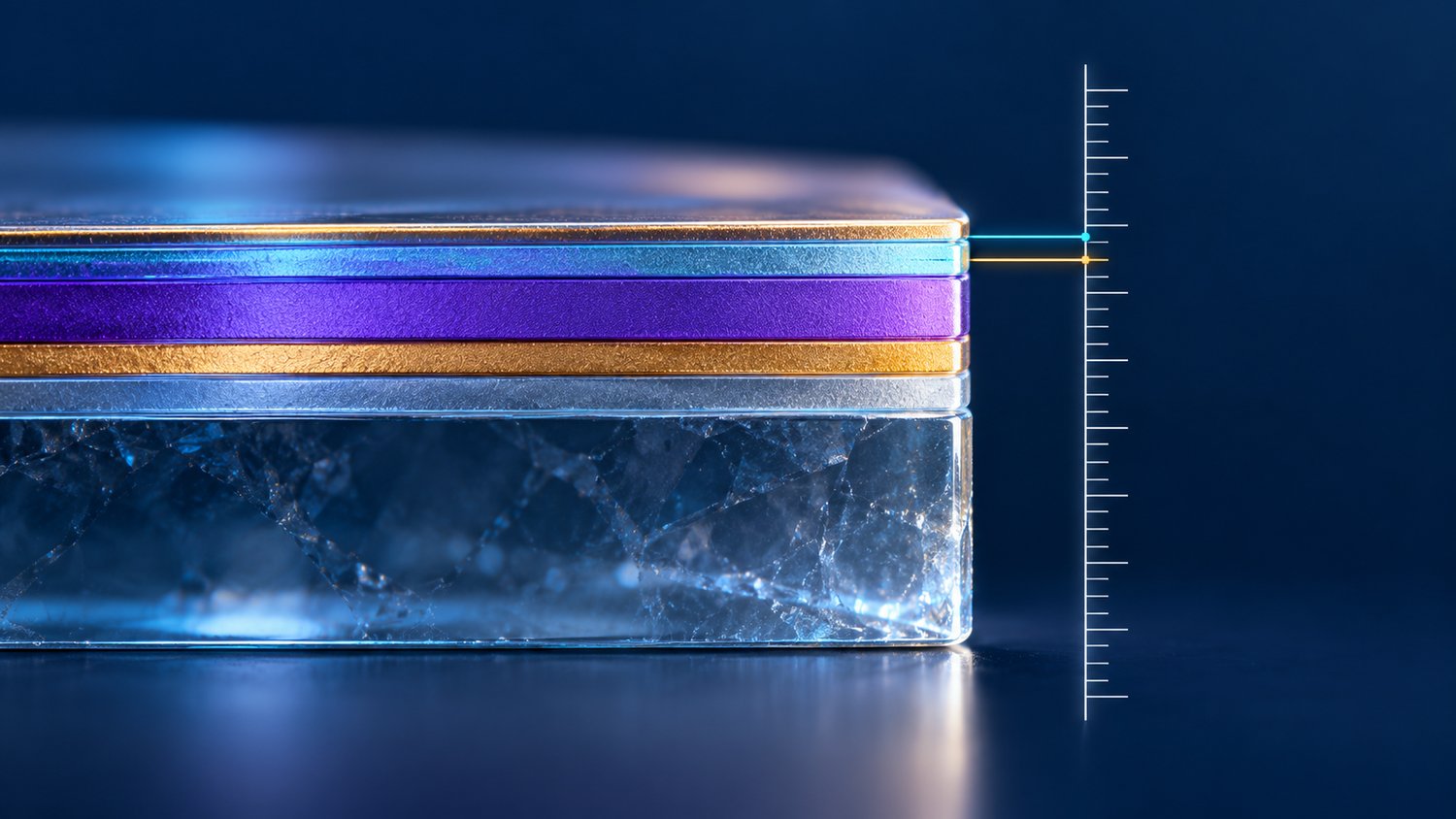
Coating thickness control keeps each deposited layer within its design tolerance. A correct total stack thickness is insufficient: opposite errors in two layers may cancel mechanically while leaving different optical phases. The relevant quantity is optical thickness, $nd$, where $n$ is refractive index and $d$ is physical thickness.
Define center wavelength (CWL), full width at half maximum (FWHM), optical density (OD), and angle of incidence (AOI) before discussing tolerances. For a filter specified at CWL 780 nm and FWHM 20 nm, “1 nm thickness accuracy” alone says little about compliance. Layer sensitivity and the pattern of errors matter.
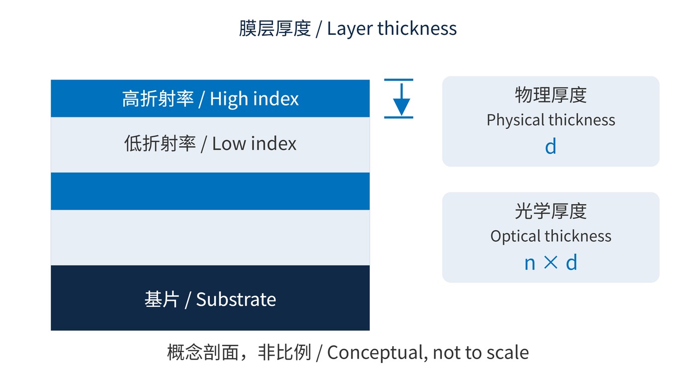
As Fig. 1 illustrates, both index and thickness set the phase. At normal incidence, the phase thickness of one layer is:
$$\delta = \frac{2\pi nd}{\lambda}$$
A quarter-wave layer at 780 nm with $n=2.10$ is $92.86\,\mathrm{nm}$ thick. Adding 1 nm changes its thickness by about 1.08%. This index is an illustrative input, rather than a universal value for a particular material.
If every layer is scaled by the same fraction, unchanged indices and negligible dispersion allow the wavelength scale to move by that fraction. A first-order optical-thickness estimate is:
$$\frac{\Delta\lambda}{\lambda_0}\approx\frac{\Delta(nd)}{nd}\approx\frac{\Delta d}{d}+\frac{\Delta n}{n}$$
A common 1% thickness increase therefore shifts a feature near 780 nm by approximately 7.8 nm toward longer wavelengths. This does not predict the effect of adding 1 nm to an arbitrary single layer. That requires the complete stack model. Index changes also affect optical thickness, so deposition time cannot explain every spectral shift.
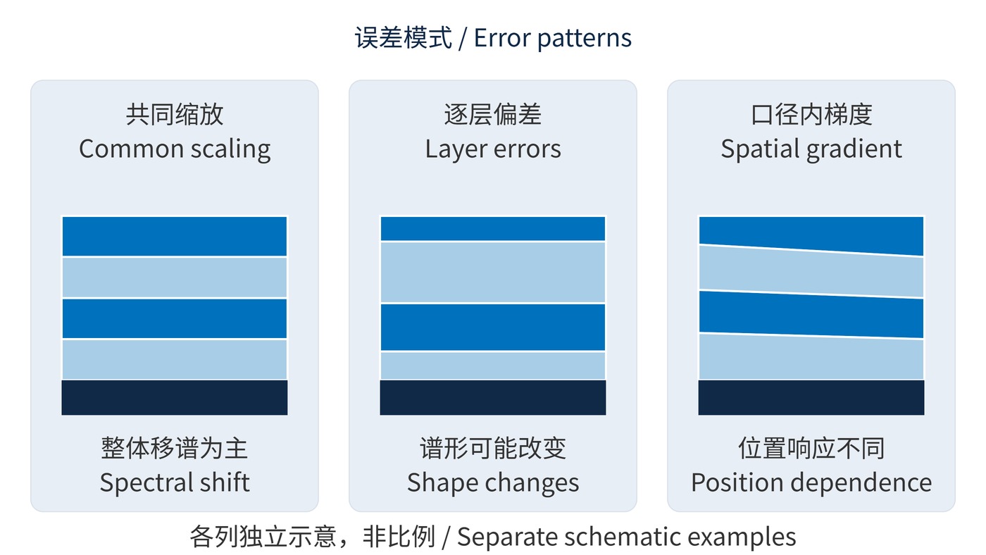
The three error patterns in Fig. 2 require separate treatment. Common scaling mainly translates the spectrum. Independent layer errors can change bandwidth, peak transmission, and leakage. A spatial gradient produces different spectra across the aperture. A single wavelength correction cannot generally remove the latter two effects.
Start with application limits. An illustrative acceptance specification might require CWL 780±1 nm, FWHM 20±2 nm, peak transmission at least 90%, and OD6 throughout 400–700 nm. These are example targets, not a product specification. OD6 means transmission no greater than 0.0001%; the measurement needs sufficient dynamic range.
Allocating the entire ±1 nm CWL allowance to common thickness scaling gives approximately ±0.128%, or ±0.119 nm for the 92.86 nm layer. This is only an upper-bound estimate under the stated assumptions. Temperature, AOI, index variation, and measurement uncertainty consume part of the allowance. It is not a valid blanket tolerance for every layer.
| Question | Evidence to request |
|---|---|
| Which layers are sensitive? | Layer perturbations evaluated against CWL, FWHM, and worst-case blocking |
| How are errors correlated? | Monte Carlo results using a realistic error model, including distributions and yield |
| Is the aperture uniform? | Spectra measured at the center and edge of the clear aperture |
| Does monitoring predict the part? | Calibration linking crystal and optical monitoring to finished-part measurements |
A quartz crystal microbalance (QCM) infers thickness from mass loading; density assumptions and the sensor-to-part tooling factor affect the result. Optical monitoring uses the growing stack’s optical response, but remains dependent on signal quality, design, and stable indices. Display resolution is not finished-part accuracy. Studies in Coatings on broadband monitoring errors, and papers in Applied Optics on optical coating monitoring, describe these distinctions.
In narrowband laser detection, check that the laser line stays inside the high-transmission region under worst-case errors. Nominal CWL is insufficient. In fluorescence detection, evaluate leakage at the excitation wavelength as well: some layer errors can compromise local blocking while CWL still passes.
Large-aperture imaging filters require spatial measurements alongside field-angle analysis. Record agreed conditions such as AOI 0° and temperature 23 °C, plus beam divergence and sampling positions. This helps distinguish coating nonuniformity from angle-dependent behavior.
When reviewing a tolerance report, ask whether the quoted value is a maximum deviation, a standard deviation, or instrument resolution. These quantities describe different things and cannot be substituted for one another in an error budget.
The practical acceptance criterion is spectral margin across the agreed aperture, angle, and temperature. A nanometer reading becomes useful only when it is demonstrably linked to that performance.
 365nm Narrow Bandpass Filter | Ø50mm | T>90%
OT-HBP3659050
365nm Narrow Bandpass Filter; FWHM 10nm; transmission >90%; blocking OD5; size Ø50mm; AOI 0°.
 450nm Narrow Bandpass Filter | Ø50mm
OT-HBP4509050
450nm Narrow Bandpass Filter; FWHM 10nm; transmission >90%; blocking OD5; size Ø50mm; AOI 0°.
 525nm Narrow Bandpass Filter | Ø50mm
OT-HBP5259050
525nm Narrow Bandpass Filter; FWHM 10nm; transmission >90%; blocking OD5; size Ø50mm; AOI 0°.
Send us your drawing and spectral targets — an engineer replies with a feasibility check and quotation within one business day.