Original content by the OOTEE Optics editorial team, drawn from first-hand production line and inspection data. Please credit the source when republishing.
Given limits in expertise and test conditions, the theories, parameters and conclusions here carry no guarantee of absolute accuracy. For technical learning and exchange only - never the sole basis for design, acceptance or selection. Corrections welcome.
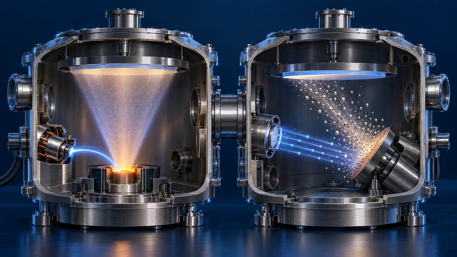
Electron beam evaporation and sputtering are physical vapor deposition (PVD) methods. Both transport source material through a vacuum chamber to build a film. Neither specifies a particular filter design: the useful comparison is how particles are generated and how that affects process control and acceptance evidence.
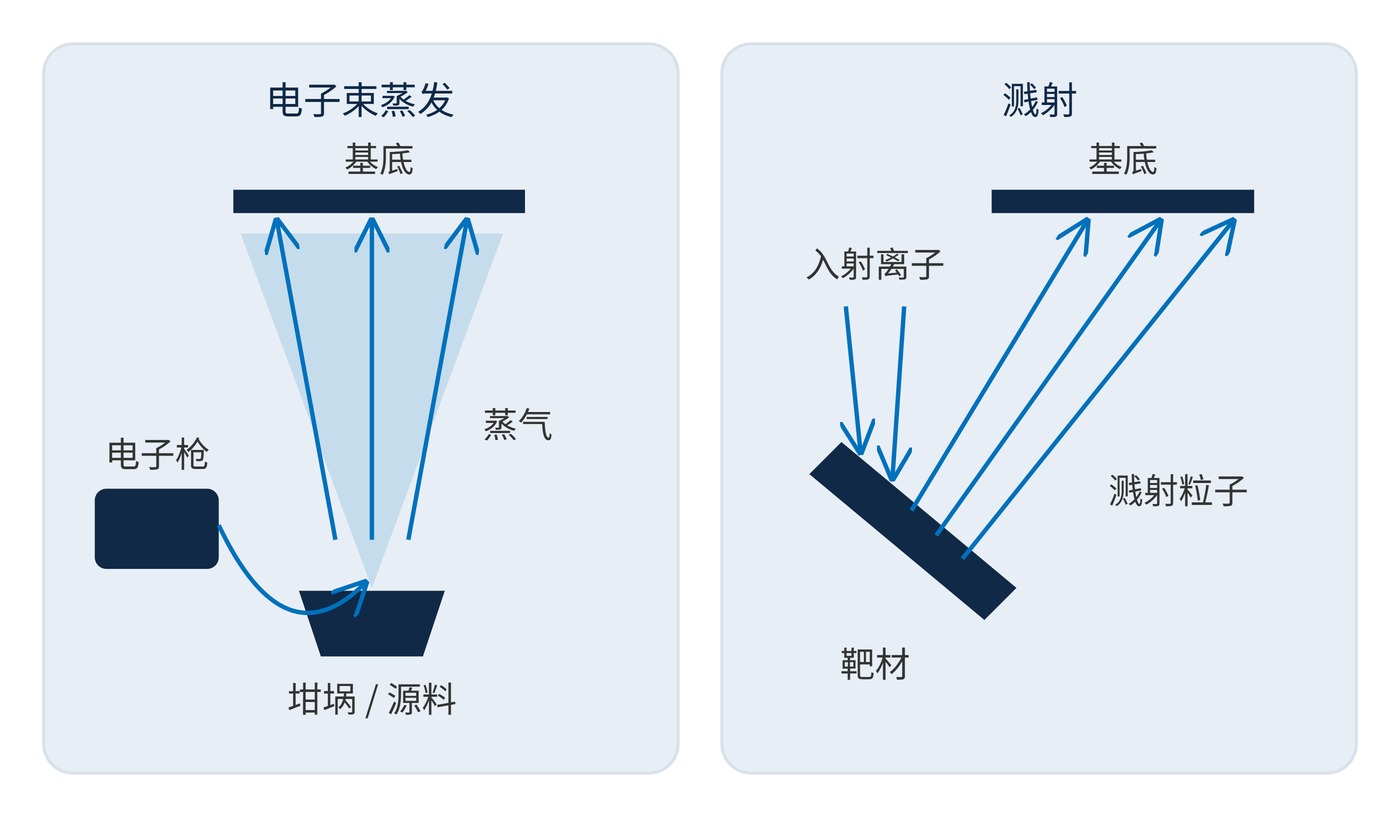
In evaporation, an electron gun heats material in a crucible; vapor travels toward a substrate and condenses. Sputtering transfers momentum from energetic ions to a target, ejecting target atoms. Fig. 1 distinguishes the two routes. The electron beam primarily heats the evaporation source, while sputtering ions primarily strike the target.
Magnetron sputtering confines electrons magnetically to sustain plasma near the target. Ion beam sputtering (IBS) uses a separate ion source. Their equipment, throughput and economics differ; specifying only “sputtered” leaves an important manufacturing distinction unresolved.
A multilayer filter selects wavelengths through phase relationships. The phase thickness of a layer is given below, where $n$ is refractive index, $d$ is physical thickness, $\theta$ is the propagation angle inside the layer, and $\lambda$ is vacuum wavelength. Controlling thickness alone is insufficient if refractive index or absorption changes.
$$\delta=\frac{2\pi n d\cos\theta}{\lambda}$$
At normal incidence, neglecting dispersion and assuming that every layer experiences the same fractional optical thickness change, the approximate spectral shift is:
$$\frac{\Delta\lambda}{\lambda}\approx\frac{\Delta(nd)}{nd}\approx\frac{\Delta n}{n}+\frac{\Delta d}{d}$$
A uniform 0.1% increase therefore suggests a red shift of about 0.78 nm near 780 nm. This is a sensitivity estimate, not a multilayer simulation. Individual layer errors can also alter passband ripple and blocking leakage.
Unassisted evaporation generally delivers lower energy particles, making film growth sensitive to substrate temperature and surface mobility. Ion assistance changes those conditions. Sputtered particles generally start with higher energies, but gas collisions modify their energy and direction. Densification must be balanced against stress, absorption and defects.
| Control task | Electron beam evaporation | Sputtering |
|---|---|---|
| Source stability | Beam position, melt behavior, rate fluctuations and spitting | Target condition, discharge stability and arc particles |
| Composition | Source decomposition, oxygen pressure and oxidation | Reactive gas control, target poisoning and stoichiometry |
| Uniformity | Monitor calibration, source distance, rotation and masks | Target erosion, geometry and substrate motion |
| Mechanical state | Thermal history and ion assistance | Pressure, power, bias and stress control |
An illustrative requirement could specify center wavelength (CWL) 780 nm, full width at half maximum (FWHM) 20 nm, peak transmission ≥90%, and optical density (OD) ≥6 over 800–1000 nm. Also state angle of incidence (AOI) 0°, measurement temperature 23 °C and clear aperture. These are example targets, not a product specification.
Compare measured spectra, spatial maps, substrate thermal limits and coating induced figure changes against the same requirements. Environmental testing needs identical before-and-after conditions and a defined recovery interval, so reversible thermal shifts are not confused with permanent changes.
For a useful comparison, keep substrate material, aperture, mounting and measurement geometry consistent. Ask whether a reported spectrum represents a production part, a witness coupon or a calculated design. Also establish whether rejection criteria apply to every measured position or only an aperture average. Averages can conceal localized leakage that matters in an imaging instrument.
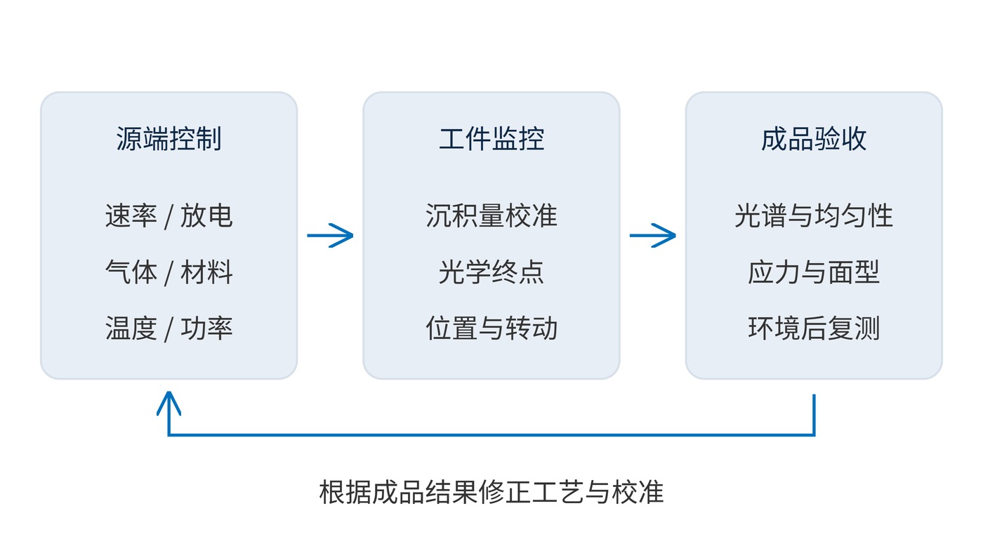
Fig. 2 links source control to finished-part acceptance. A quartz crystal monitor tracks deposited material; optical monitoring tracks the evolving optical response. Both require calibration to the workpiece. A passing witness sample cannot establish compliance across the entire clear aperture.
Fluorescence instruments need deep blocking and low background. Check measurement dynamic range, stray light and pinholes: an OD6 requirement does not establish that a spectrometer can verify OD6. Compact imaging systems may instead be limited by coating stress and spectral behavior over the actual illumination cone.
Large apertures and multi-part loads require spatial and load-position mapping. Temperature-sensitive substrates need a complete thermal budget, rather than a heater setpoint. For small production runs, compare material changes, cleaning, setup and yield alongside deposition time; rate alone does not determine unit cost.
Qualification should therefore follow the application risk. A stable average spectrum cannot compensate for an unacceptable local defect, and a flat substrate before coating does not establish its final figure. Retain the relevant measurement conditions with each result so later batches can be compared meaningfully.
Judge either route using spectra, uniformity, mechanical behavior and environmental retesting under matched conditions. The process name describes how the coating was made; measurement establishes whether it meets its intended use.
Technical references: thin-film deposition facility notes published by the ASU nanofabrication center, and deposition technical notes from vacuum-equipment suppliers such as Lesker.
 365nm Narrow Bandpass Filter | Ø50mm | T>90%
OT-HBP3659050
365nm Narrow Bandpass Filter; FWHM 10nm; transmission >90%; blocking OD5; size Ø50mm; AOI 0°.
 450nm Narrow Bandpass Filter | Ø50mm
OT-HBP4509050
450nm Narrow Bandpass Filter; FWHM 10nm; transmission >90%; blocking OD5; size Ø50mm; AOI 0°.
 525nm Narrow Bandpass Filter | Ø50mm
OT-HBP5259050
525nm Narrow Bandpass Filter; FWHM 10nm; transmission >90%; blocking OD5; size Ø50mm; AOI 0°.
Send us your drawing and spectral targets — an engineer replies with a feasibility check and quotation within one business day.