Original content by the OOTEE Optics editorial team, drawn from first-hand production line and inspection data. Please credit the source when republishing.
Given limits in expertise and test conditions, the theories, parameters and conclusions here carry no guarantee of absolute accuracy. For technical learning and exchange only - never the sole basis for design, acceptance or selection. Corrections welcome.
An interference thin-film filter uses a sequence of dielectric layers to control how optical fields combine. Alternating high and low refractive indices create many partially reflecting interfaces. Their combined response sends selected wavelengths back toward the source while allowing others through.
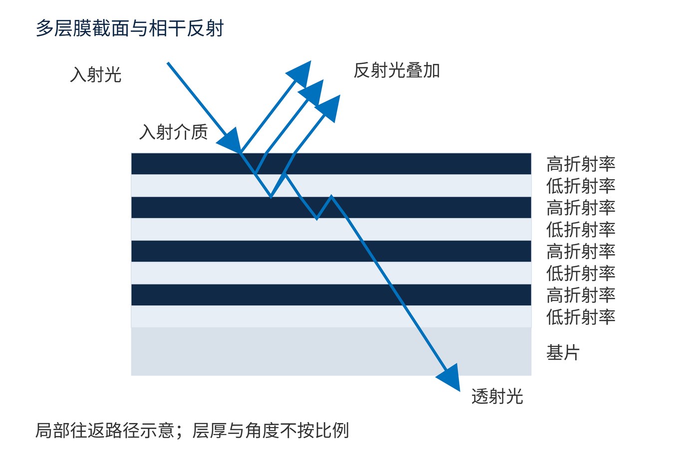
As Fig. 1 shows, the outgoing fields include contributions from multiple reflections inside the coating. Field amplitudes interfere; interface reflectances cannot simply be added. A low-loss blocking coating mainly reflects rejected energy, so the instrument must provide a suitable path for that returned light.
For a layer of physical thickness $d$ and refractive index $n$, the one-way phase thickness is:
$$\delta=\frac{2\pi nd\cos\theta}{\lambda}$$
Here $\theta$ is the angle inside that layer and $\lambda$ is the vacuum wavelength. Reflection phase must also enter the interference condition. For two paths differing by a round trip through a layer:
$$2\delta+\Delta\phi_{\mathrm{r}}=2m\pi\quad\Longleftrightarrow\quad 2nd\cos\theta=\left(m-\frac{\Delta\phi_{\mathrm{r}}}{2\pi}\right)\lambda$$
The integer $m$ labels the order; $\Delta\phi_{\mathrm{r}}$ is the net reflection-phase difference. The familiar $2nd\cos\theta=m\lambda$ applies when that phase difference vanishes or can be absorbed into the order. A complete multilayer requires a calculation across all interfaces.
At normal incidence, a quarter-wave stack satisfies $n_{\mathrm{H}}d_{\mathrm{H}}=n_{\mathrm{L}}d_{\mathrm{L}}=\lambda_0/4$. Each layer contributes a one-way phase of $\pi/2$. Propagation and reflection phases make the reflected fields reinforce near $\lambda_0$. For a lossless $(\mathrm{HL})^N$ stack, starting at the incident side and ending on a substrate:
$$R_N(\lambda_0)=\left[\frac{n_{\mathrm{s}}(n_{\mathrm{H}}/n_{\mathrm{L}})^{2N}-n_0}{n_{\mathrm{s}}(n_{\mathrm{H}}/n_{\mathrm{L}})^{2N}+n_0}\right]^2$$
$N$ counts layer pairs, while $n_0$ and $n_{\mathrm{s}}$ describe the incident medium and substrate. With indices 2.10 and 1.45, air incidence and a substrate index of 1.52, the ideal center reflectance rises from about 87.3% for 4 pairs to 99.96% for 12 pairs. This is the result of coherent field addition.
For an infinite, nondispersive quarter-wave structure at normal incidence, the fractional stopband width in frequency is:
$$\frac{\Delta\nu}{\nu_0}=\frac{4}{\pi}\arcsin\left(\frac{n_{\mathrm{H}}-n_{\mathrm{L}}}{n_{\mathrm{H}}+n_{\mathrm{L}}}\right)$$
The example gives approximately 23.4%. Replacing this with a fractional wavelength width is only a narrow-band approximation. Index contrast sets the underlying gap width; more pairs deepen rejection and alter the finite stack's edge and ripple. Practical sharp-edge coatings also use thickness optimization and matching layers.
Fig. 2 uses a characteristic-matrix calculation to compare identical materials and design wavelength at different pair counts. The passband oscillations remain visible. Substrate-backside effects, absorption, dispersion and fabrication errors are excluded; these are calculated illustrations, not measured product spectra.
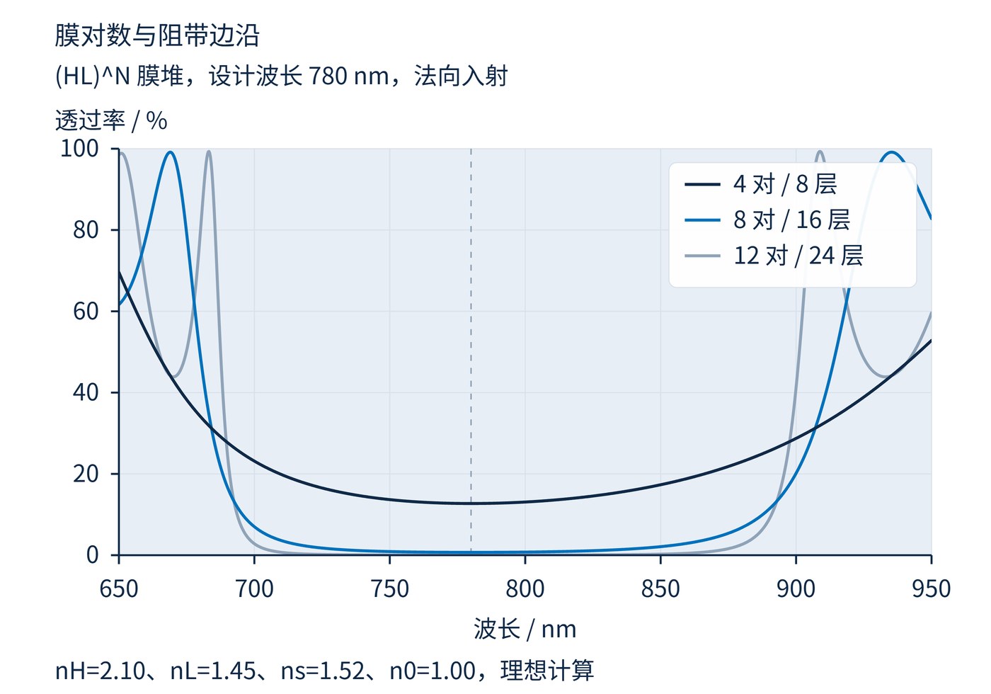
At a 780 nm reference wavelength, the high and low index layers in this example are approximately 92.9 nm and 134.5 nm thick. Different physical thicknesses therefore give the same optical thickness. Scaling every optical thickness by the same factor shifts the principal spectral features; independent layer errors instead disturb the phase relationships and reshape the response.
The stack reference $\lambda_0$ need not equal the finished filter's center wavelength (CWL). A bandpass design can place cavity layers between reflecting stacks to create a transmission resonance. Its full width at half maximum (FWHM) is not the stopband width calculated above.
Separate nominal design values, typical measured curves and guaranteed acceptance limits. If useful and unwanted wavelengths are close together, a normal-incidence collimated spectrum may be insufficient: the system illuminates the coating over a distribution of angles. Temperature also changes refractive index and physical thickness, so sample measurements should use the specified thermal conditions.
For a bandpass filter, define the bandwidth convention explicitly. FWHM is measured between the two wavelengths at half the peak transmission; it does not establish a flat usable passband or a guaranteed minimum within it. Likewise, a blocking requirement needs both wavelength limits, rather than a single impressive OD value at one wavelength.
Fluorescence optics combine excitation rejection with a cavity-defined emission window. Laser beam routing uses complementary reflection and transmission, with attention to returned light. Vision systems place an optimized longpass or shortpass edge between useful signal and unwanted background.
These functions share a phase-control mechanism but require different designs. A single periodic stack creates a finite reflection band; broad ultraviolet-to-near-infrared blocking needs additional design measures.
A cavity is a phase-control region between reflecting stacks. At resonance, repeated round trips reinforce transmission through that region while the surrounding coating supplies rejection. Coupling multiple cavities can flatten the transmission window and sharpen its sides, but it also makes layer tolerances more consequential. The simple periodic mirror remains a building block rather than a complete recipe for every spectral shape.
For broadband backgrounds, compare the full blocking range with the detector response. A remote transmission window can admit unwanted energy even when the principal rejection band is deep. The acceptance spectrum must therefore cover the wavelengths the detector can actually register, not only the immediate neighborhood of the intended passband.
Layer count alone does not establish quality. Extra layers can increase sensitivity to thickness errors and complicate stress control, while passband ripple may remain. Neither a center reflectance value nor a simple sum of interface reflectances establishes rejection over an entire interval.
Evaluate the complete design at the operating angles, including fabrication tolerances. Compare nominal performance with the specified limits across the full wavelength interval, rather than judging the coating from its design point alone. The useful result is the worst-case combination of transmission, rejection and edge position that the optical system can accept.
 365nm Narrow Bandpass Filter | Ø50mm | T>90%
OT-HBP3659050
365nm Narrow Bandpass Filter; FWHM 10nm; transmission >90%; blocking OD5; size Ø50mm; AOI 0°.
 450nm Narrow Bandpass Filter | Ø50mm
OT-HBP4509050
450nm Narrow Bandpass Filter; FWHM 10nm; transmission >90%; blocking OD5; size Ø50mm; AOI 0°.
 525nm Narrow Bandpass Filter | Ø50mm
OT-HBP5259050
525nm Narrow Bandpass Filter; FWHM 10nm; transmission >90%; blocking OD5; size Ø50mm; AOI 0°.
Send us your drawing and spectral targets — an engineer replies with a feasibility check and quotation within one business day.