Original content by the OOTEE Optics editorial team, drawn from first-hand production line and inspection data. Please credit the source when republishing.
Given limits in expertise and test conditions, the theories, parameters and conclusions here carry no guarantee of absolute accuracy. For technical learning and exchange only - never the sole basis for design, acceptance or selection. Corrections welcome.
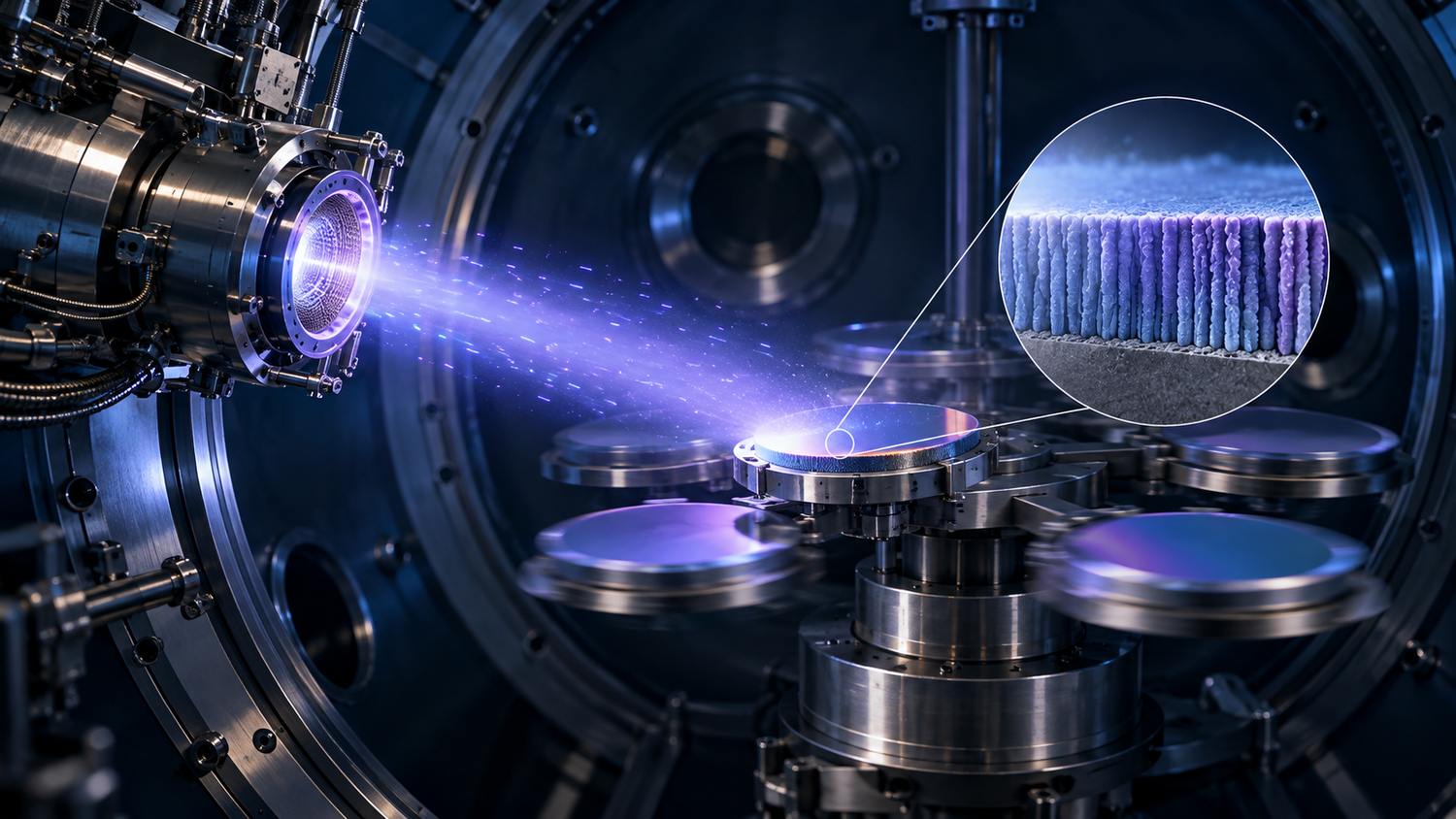
Ion-assisted deposition (IAD) adds an energetic ion flux while coating material condenses onto a substrate. In a typical evaporation system, the evaporator supplies the film material and a separate ion source supplies energy and momentum. The assistance acts during growth; it is neither a final compression step nor another name for ion-beam sputtering.
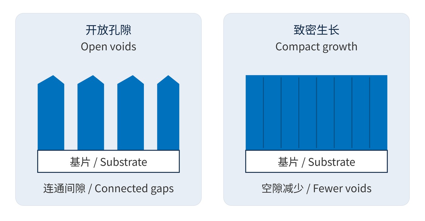
At low substrate temperatures, arriving species may have too little mobility to find compact arrangements. Protrusions shadow neighbouring areas, leaving open spaces between columns. Ion assistance can change this growth pathway before the next material buries the surface. Adding thickness alone does not provide the same mechanism.
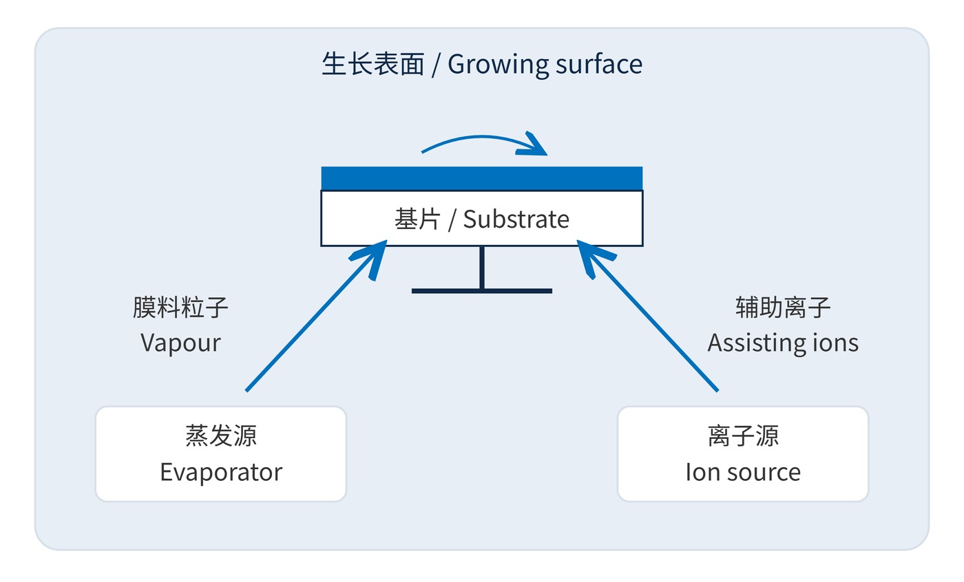
Fig. 1 separates the material supply from the assisting beam. Suitable bombardment promotes surface rearrangement and reduces shadowing. For oxides, the reactive atmosphere also helps control composition. Substrate rotation averages exposure, but cannot by itself guarantee uniform ion and vapour fluxes over every holder position.
Source voltage alone is an incomplete process specification. Consider ion energy $E_i$, ion arrival flux $J_i$, depositing-species flux $J_a$, and substrate temperature together. A useful comparison metric for recipes on the same equipment is:
$$\varepsilon = E_i\frac{J_i}{J_a}$$
This is incident energy per arriving film-forming species, not the energy each atom actually absorbs. For an illustrative $E_i=100\,\mathrm{eV}$ and $J_i/J_a=0.2$, the metric is $20\,\mathrm{eV}$ per arriving species. These values are an arithmetic example, not a process recommendation. Raising deposition rate at fixed ion flux lowers the ratio. Ion mass, energy distribution and direction still matter, so matching this number does not make two sources equivalent.
Fig. 2 illustrates connected voids rather than measured morphology. A dense oxide may remain amorphous: densification does not require larger crystals. X-ray reflectivity fitting can help assess density, provided composition, roughness and model uncertainty are considered.
Reducing void content often moves refractive index toward the dense-material value and restricts pathways for water uptake. Spectral features depend on optical thickness $nd$. For a fixed interference order near normal incidence, with approximately common fractional changes across the stack, small changes can be understood through:
$$\frac{\Delta\lambda}{\lambda}\approx\frac{\Delta n}{n}+\frac{\Delta d}{d}$$
An index increase of 0.1% alone would move a 780 nm feature by about 0.78 nm. Densification may also change physical thickness. This estimate therefore does not replace a multilayer calculation using measured optical constants for the chosen recipe. Excessive bombardment can introduce resputtering, composition changes, absorbing defects and unwanted stress.
Define centre wavelength (CWL), full width at half maximum (FWHM), optical density (OD), and angle of incidence (AOI) before specifying a process. An example requirement is CWL 780 nm, FWHM 20 nm and AOI 0°, with OD6 blocking over 400–700 nm. This is a hypothetical specification, not a product claim.
| Concern | Evidence to request |
|---|---|
| Spectral stability | Before-and-after CWL, bandwidth and transmission at matching positions, with exposure and recovery conditions |
| Film density | Density or porosity-sensitive measurements on run-matched witnesses, including fitting assumptions |
| Stress and deformation | Curvature or figure change on the intended substrate thickness, with coating side and support defined |
| Loss and uniformity | Absorption, scatter and holder-position sampling in the required band, with instrument dynamic range |
OD6 means a transmitted fraction of $10^{-6}$. An ordinary transmission instrument's noise floor cannot establish compliance. Recipe comparisons should hold material, stack, substrate and measurement conditions constant. A higher refractive index alone is insufficient proof of greater density because composition can also change the index.
Ask whether witness samples represent the same exposure as the optics being purchased. A stationary witness near the chamber wall may receive a different ion-to-material ratio from a rotating production part. Acceptance limits should also distinguish permanent changes from reversible shifts after samples return to the agreed measurement environment.
For narrowband imaging and fluorescence detection, compact films can reduce changes in optical thickness following environmental exposure. The delivered assembly still needs passband and excitation-rejection verification. Thick multilayers require stress control as well: a satisfactory spectrum does not ensure an undistorted imaging substrate.
On temperature-sensitive substrates, ion assistance can reduce reliance on bulk heating. The beam nevertheless supplies heat, so actual substrate temperature must be recorded. UV and high-power applications also need absorption, defect and laser-damage measurements; density alone cannot establish a performance rating.
The coupled roles of ion energy and arrival ratio are covered extensively in the thin-film growth literature and are not expanded here. Qualification should connect density measurements with optical loss, stress and spectra measured before and after environmental exposure.
 365nm Narrow Bandpass Filter | Ø50mm | T>90%
OT-HBP3659050
365nm Narrow Bandpass Filter; FWHM 10nm; transmission >90%; blocking OD5; size Ø50mm; AOI 0°.
 450nm Narrow Bandpass Filter | Ø50mm
OT-HBP4509050
450nm Narrow Bandpass Filter; FWHM 10nm; transmission >90%; blocking OD5; size Ø50mm; AOI 0°.
 525nm Narrow Bandpass Filter | Ø50mm
OT-HBP5259050
525nm Narrow Bandpass Filter; FWHM 10nm; transmission >90%; blocking OD5; size Ø50mm; AOI 0°.
Send us your drawing and spectral targets — an engineer replies with a feasibility check and quotation within one business day.