Original content by the OOTEE Optics editorial team, drawn from first-hand production line and inspection data. Please credit the source when republishing.
Given limits in expertise and test conditions, the theories, parameters and conclusions here carry no guarantee of absolute accuracy. For technical learning and exchange only - never the sole basis for design, acceptance or selection. Corrections welcome.
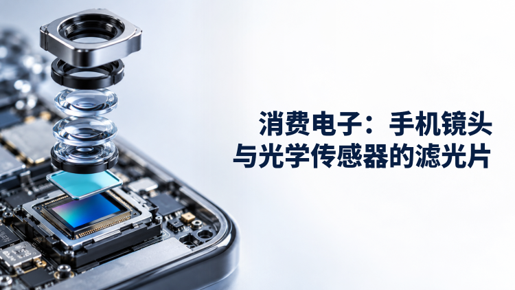
A smartphone filter is a spectral interface between optics and detector packaging. An infrared-cut filter (IR-Cut) suppresses near-infrared light in a color camera, while a depth receiver may deliberately transmit it. Similar outlines do not make these parts interchangeable. Here the engineering question is how the plate fits, survives assembly and remains consistent in production.
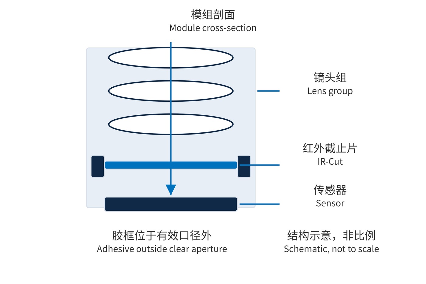
Figure 1 shows a common arrangement: lens group, IR-Cut and sensor. Other designs integrate filtering into a package window. Thickness, refractive index and mounting height belong in the optical prescription; changing the glass can shift focus even when the footprint stays identical.
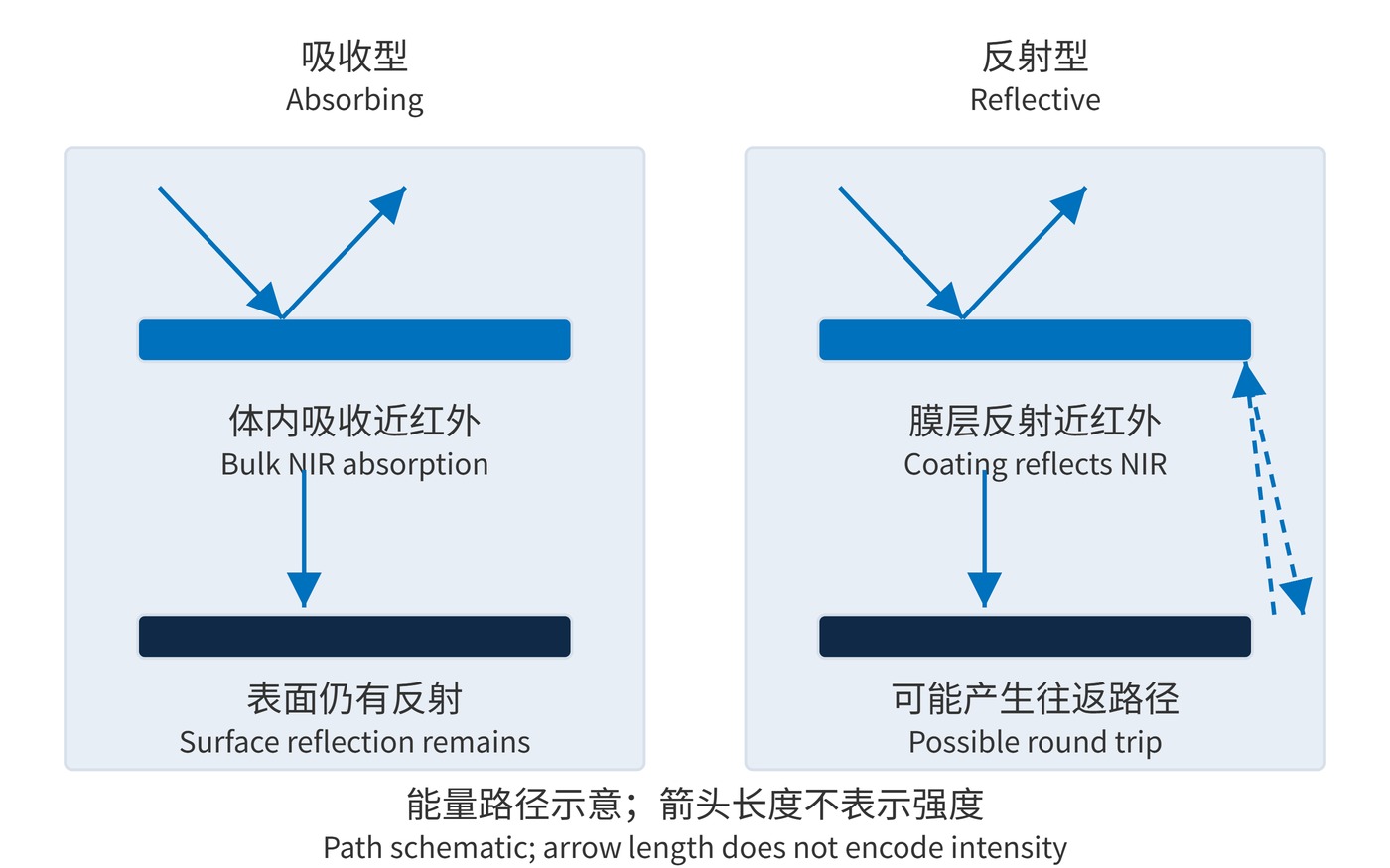
Blue absorbing glass attenuates near-infrared light within its bulk. A reflective IR-Cut redirects it with a multilayer coating; hybrid designs combine both mechanisms. Absorption depends on material and thickness, whereas an interference edge is particularly sensitive to angle of incidence (AOI). Absorbing glass still has reflecting surfaces and may need antireflection coatings.
Figure 2 traces a possible return path between sensor and filter. Absorption can weaken near-infrared recirculation, but it cannot eliminate visible surface reflections. A review of smartphone imaging technology discusses filter-related ghosts. Their strength and position depend on wavelength, reflectance, spacing and ray geometry. Material choice therefore needs a module-level bright-source test rather than a simple absorbing-versus-reflecting ranking.
Optical density (OD) uses fractional transmittance $T$. OD4 means 0.01% transmission at the stated wavelength. Acceptance criteria must also define the blocking interval and measurement stray-light floor.
$$\mathrm{OD}(\lambda)=-\log_{10}T(\lambda)$$
For a narrow bandpass, specify center wavelength (CWL), full width at half maximum (FWHM) and peak transmission. The following effective-index approximation estimates angular blue shift; actual cones and polarization require measurement.
$$\lambda(\theta)\approx\lambda(0)\sqrt{1-\frac{\sin^2\theta}{n_{\mathrm{eff}}^2}}$$
With $n_{\mathrm{eff}}=1.9$, a 940 nm normal-incidence center moves to approximately 925 nm at 20°. A 15 nm shift matters for a 20 nm FWHM passband, so a normal-incidence trace alone is insufficient.
Start with the emitter wavelength envelope over temperature, receiver field and ray cone. When comparing narrow bandpass filters, a discussion example is CWL 940 nm, FWHM 20 nm, peak transmission ≥90% and OD4 across 400–850 nm and 1000–1100 nm. These are illustrative targets, not a universal phone specification; transition regions need separate limits.
| Constraint | Drawing or acceptance requirement |
|---|---|
| Mechanical fit | Example: 4 mm × 4 mm, thickness 0.21 ±0.01 mm; adhesive area, clear aperture and orientation |
| Operating envelope | Passband envelope at AOI 0–20° and −20 to 85 °C; confirm actual system limits |
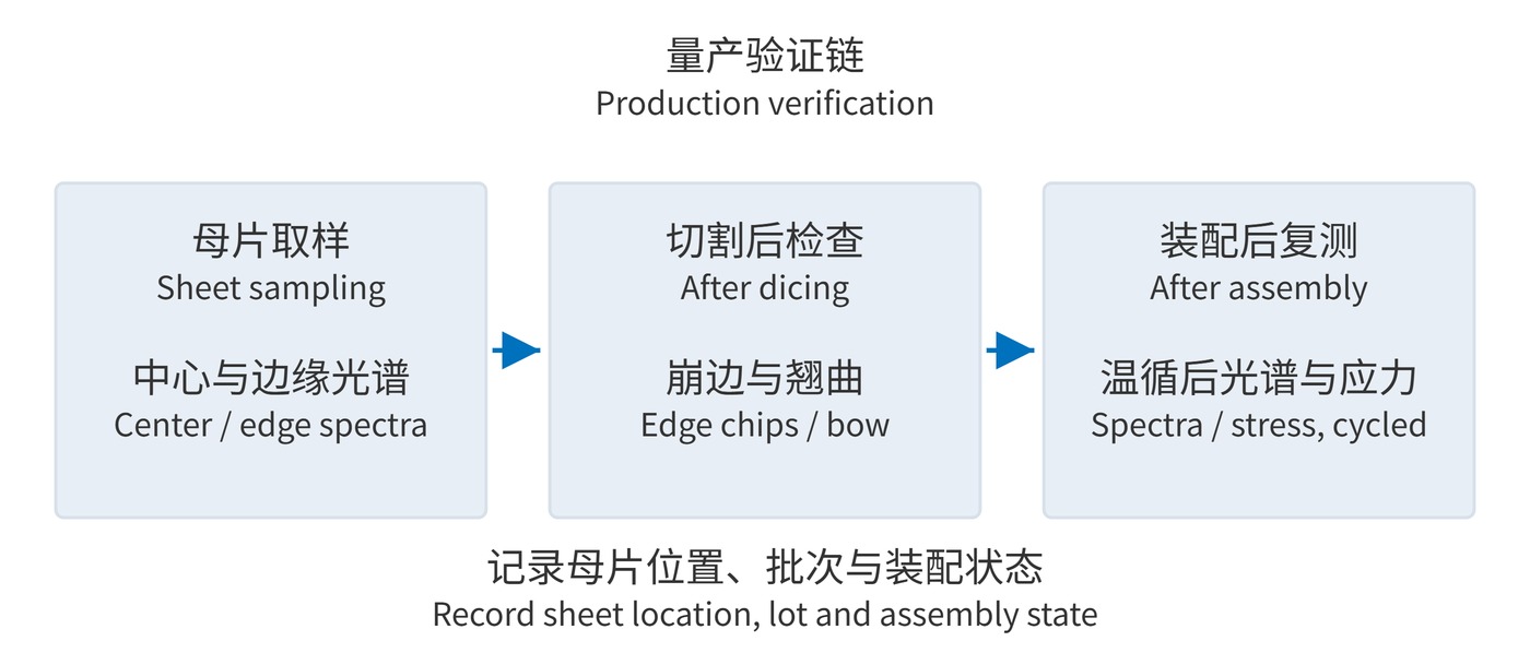
| Production control | Center/edge spectra, chip limits, bow, cleanliness and post-assembly test method |
Small dimensions do not guarantee low stress. Plate bending stiffness scales approximately with thickness cubed; coating stress, cut-edge defects and adhesive shrinkage can produce bow. Test both free and bonded parts. Figure 3 follows sampling across parent-sheet locations and assembly stages.
The adhesive footprint should remain outside the clear aperture, and the drawing should identify which face points toward the sensor. Keep the mechanical datum and test fixture consistent between suppliers and assembly inspection. A spectrum taken from an unconstrained plate cannot, by itself, establish the condition of that plate after bonding.
Budget emitter and filter drift together. A locally linear filter model is shown below; obtain its coefficient experimentally and assess mounting stress separately.
$$\Delta\lambda_{\mathrm{CWL}}\approx k_{\mathrm{f}}\Delta T$$
Color cameras combine thin packaging, oblique rays and stringent stray-light control. The distinction between colored glass and thin-film filters is useful, but module qualification must add bonding, positional tolerances and bright-source ghost tests.
Structured-light receivers transmit the projected pattern wavelength. Time-of-flight (ToF) receivers transmit the modulated return while rejecting out-of-band ambient light. Neither removes sunlight within the passband or fixes transmitter-to-receiver window crosstalk; optical isolation remains necessary.
An ambient light sensor (ALS) generally needs a visible response weighted toward human photopic sensitivity, with infrared suppression. An example device datasheet describes wafer-level optical filtering for this purpose. Combined proximity devices may use a separate infrared channel. Substituting a 940 nm bandpass for the visible channel changes the measurement. Treat the visible and infrared paths as distinct requirements, even when they share a small package or an external window.
Release criteria should bind spectral conditions to mechanical datums and assembly state, with transmission, bow and stray-light margins verified after thermal cycling.
 365nm Narrow Bandpass Filter | Ø50mm | T>90%
OT-HBP3659050
365nm Narrow Bandpass Filter; FWHM 10nm; transmission >90%; blocking OD5; size Ø50mm; AOI 0°.
 450nm Narrow Bandpass Filter | Ø50mm
OT-HBP4509050
450nm Narrow Bandpass Filter; FWHM 10nm; transmission >90%; blocking OD5; size Ø50mm; AOI 0°.
 525nm Narrow Bandpass Filter | Ø50mm
OT-HBP5259050
525nm Narrow Bandpass Filter; FWHM 10nm; transmission >90%; blocking OD5; size Ø50mm; AOI 0°.
Send us your drawing and spectral targets — an engineer replies with a feasibility check and quotation within one business day.