Original content by the OOTEE Optics editorial team, drawn from first-hand production line and inspection data. Please credit the source when republishing.
Given limits in expertise and test conditions, the theories, parameters and conclusions here carry no guarantee of absolute accuracy. For technical learning and exchange only - never the sole basis for design, acceptance or selection. Corrections welcome.

Microscopic surface inspection locates scratches, digs, edge chips and coating anomalies on a filter. Its purpose is to identify the affected face and characterize the defect before applying an acceptance rule. It complements spectral and figure measurements. The notation itself is explained in Scratch-Dig surface quality; the focus here is a repeatable inspection procedure.
Under the MIL-PRF-13830B comparison method, the first number in 60-40 or 40-20 describes scratch visibility relative to reference standards. It is not a scratch width in micrometres. The second number specifies dig diameter in hundredths of a millimetre. Acceptance also depends on the applicable length, quantity, distribution and aperture rules.
Neither grade defines a universal threshold for unaided vision. A fine scratch may flash brightly under grazing light yet disappear under diffuse illumination. Consequently, “visible to the eye” and “fails 40-20” are different judgments.
In Fig. 1, specular reflection misses the objective while defect-scattered light enters it. This produces a bright feature against a dark background. Oblique illumination is only darkfield when the specular beam remains outside the collection cone. Rotate the specimen or illumination azimuth to reveal direction-sensitive scratches.
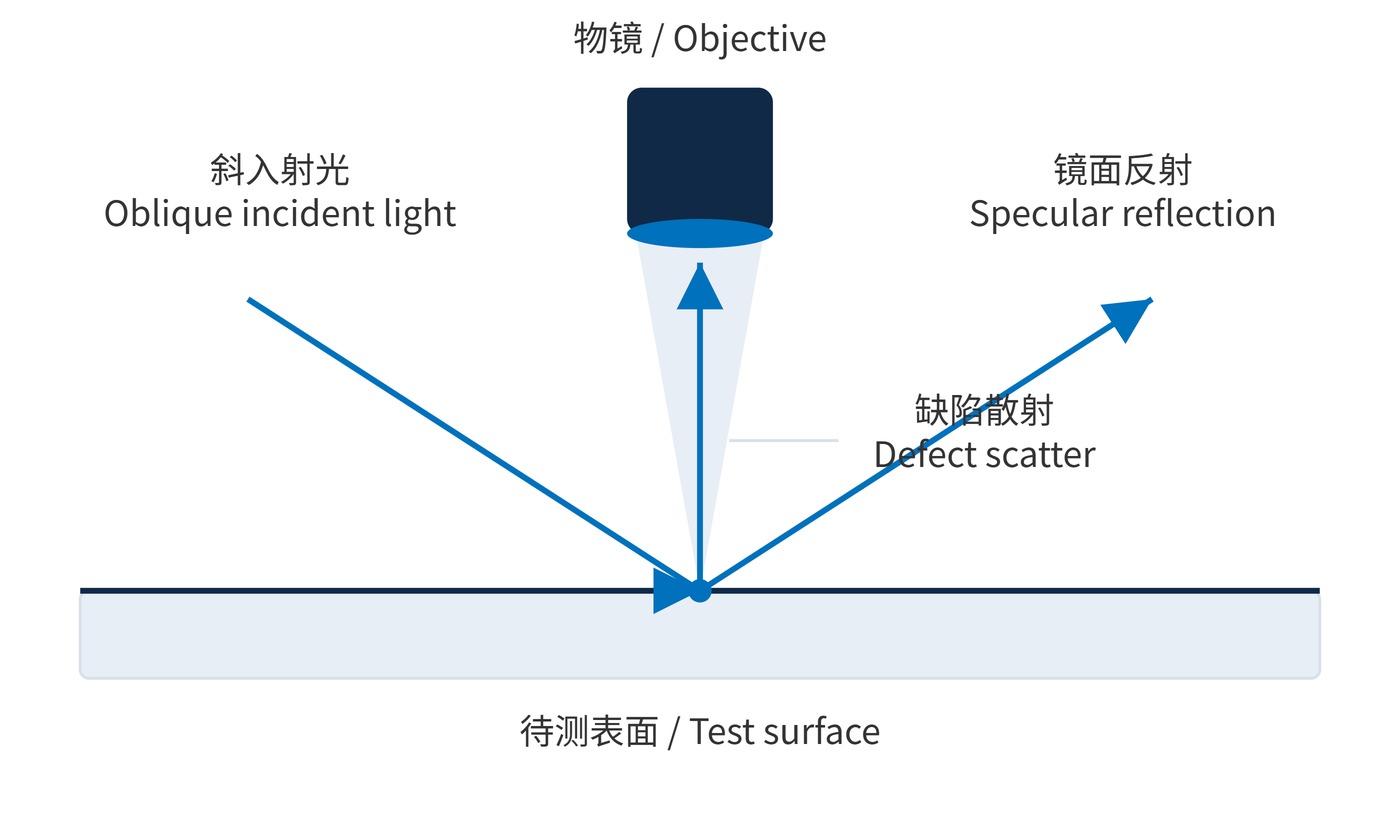
A practical starting procedure uses 5×–10× total magnification for searching and 20×–40× for classification. These are process suggestions, not prescribed acceptance magnifications. Record the objective, numerical aperture (NA), exposure and lighting direction. Diffraction, defocus and saturation can broaden a bright line, so its apparent width is not the physical scratch width.
Calibrate dimensional imaging with a stage micrometer. If a reference length $L$ spans $N$ pixels and a defect spans $n$ pixels, the object-space scale and dimension are:
$$s=\frac{L}{N},\qquad d=ns$$
A 1.00 mm reference spanning 1000 pixels gives 0.20 mm for 200 pixels. This conversion requires unchanged imaging settings and resolvable boundaries. For an irregular dig, apply the dimensional definition required by the contract; the MIL method uses:
$$d_{\mathrm{avg}}=\frac{d_{\mathrm{max}}+d_{\mathrm{min}}}{2}$$
Define the standard and edition, grade for each face, clear aperture, edge exclusion, illumination and reference set. Include rules for accumulated scratch length and clustered defects. ISO 10110-7:2017 supports specifications based on affected area or visibility; their numerical limits are not interchangeable.
| Grade | Scratch assessment | Maximum dig size | Unaided observation |
|---|---|---|---|
| 60-40 | Compare with grade 60 reference | 0.40 mm average diameter | May be visible in side lighting |
| 40-20 | Compare with grade 40 reference | 0.20 mm average diameter | May still be visible |
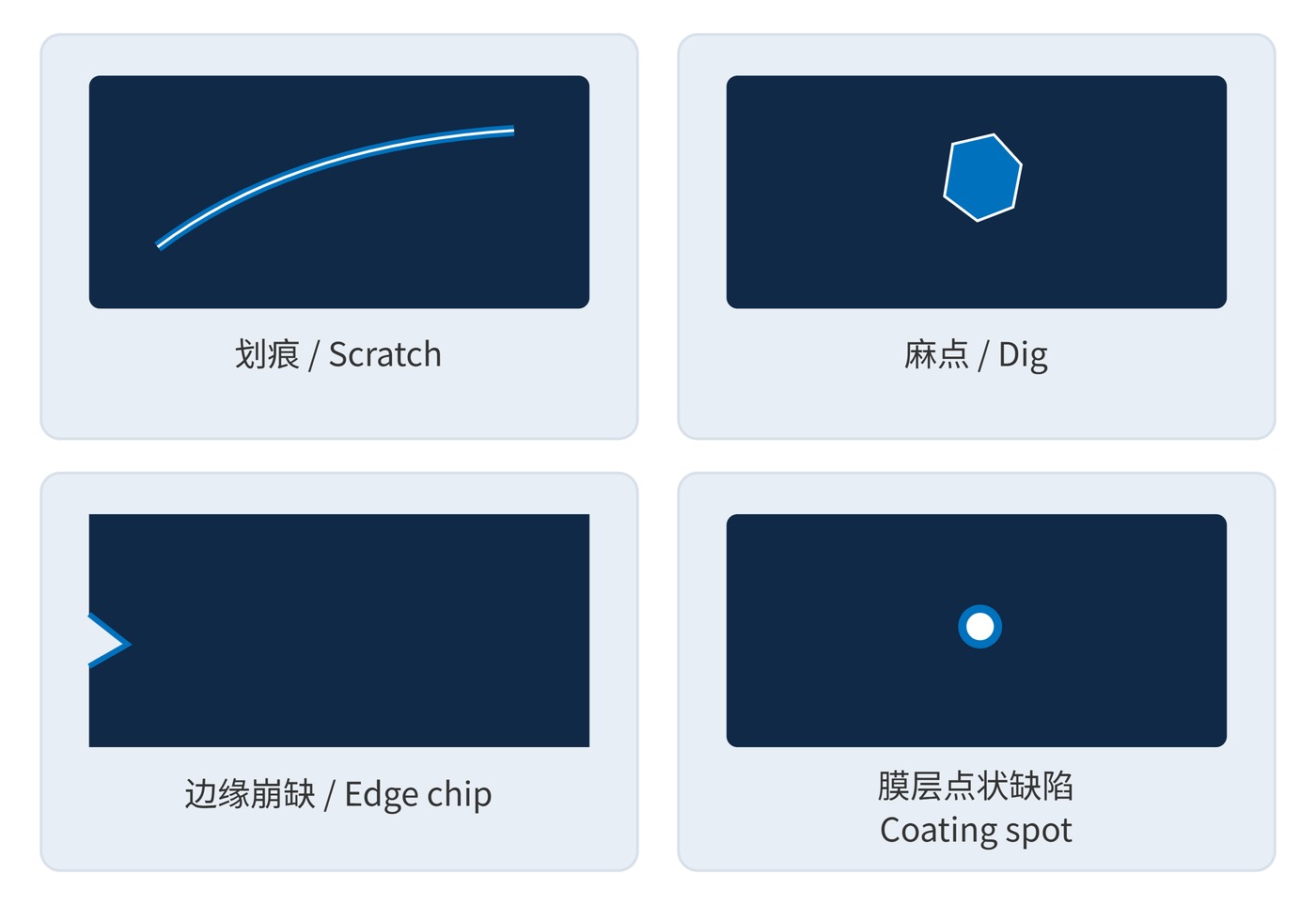
These diameters explain the dig numbers, not a permissible defect count. Inspect the reference and surface under the specified conditions rather than grading screenshot brightness. Fig. 2 separates four useful morphological categories; a coating spot must first be distinguished from contamination.
For borderline features, retain the original image alongside the dimensional calibration and avoid changing contrast between specimens. A photograph documents position and morphology, but does not preserve the viewing geometry of a reference comparison. If a second inspector reaches a different grade, repeat the observation with the same reference, lamp arrangement and sample orientation before changing the acceptance decision. Coating anomalies should also remain identified separately from substrate defects in the inspection record, even when both are assessed against the same nominal grade.
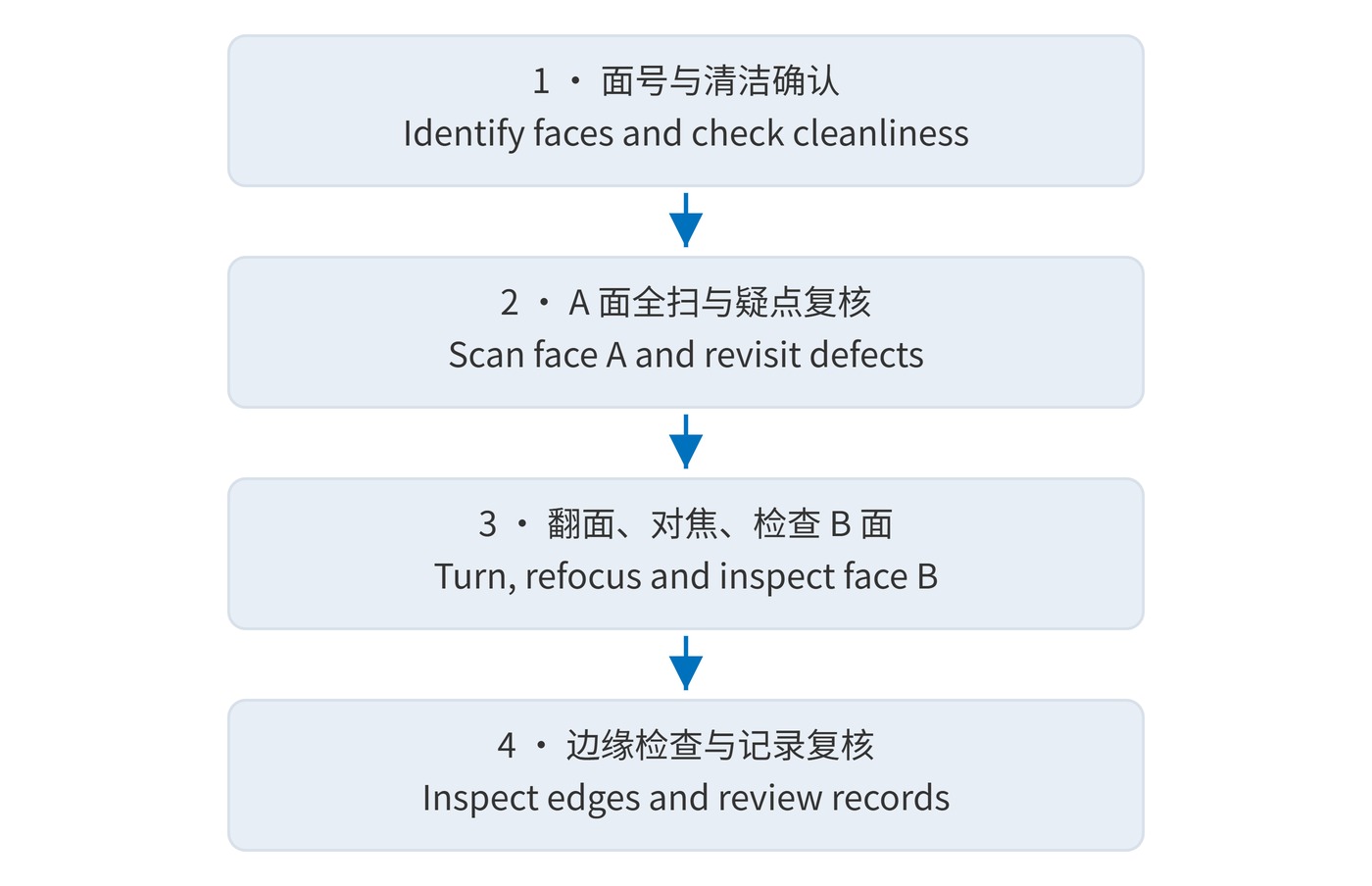
Inspect double-coated parts before assembly using the sequence in Fig. 3. Handle non-optical edges and remove dust by an approved procedure. Recheck persistent features before recording them as suspected defects; repeated wiping can introduce scratches.
For machine vision filters near an image plane, local defects may produce resolved artifacts. Weak-signal instruments also need scatter assessment. Suspected coating pinholes require transmission or imaging tests in the relevant spectral band to establish out-of-band leakage.
Higher magnification reduces field size and depth of field, making complete scanning harder. Scan the entire aperture first. Edge damage also needs review when it reaches the working aperture or includes cracks; an exclusion zone does not automatically permit every chip.
Scratch-Dig acceptance does not establish roughness, laser damage threshold or spectral blocking performance. A reproducible inspection record combines face identification, a defect map, lighting conditions, the comparison basis and review results so another inspector can repeat the decision.
 365nm Narrow Bandpass Filter | Ø50mm | T>90%
OT-HBP3659050
365nm Narrow Bandpass Filter; FWHM 10nm; transmission >90%; blocking OD5; size Ø50mm; AOI 0°.
 450nm Narrow Bandpass Filter | Ø50mm
OT-HBP4509050
450nm Narrow Bandpass Filter; FWHM 10nm; transmission >90%; blocking OD5; size Ø50mm; AOI 0°.
 525nm Narrow Bandpass Filter | Ø50mm
OT-HBP5259050
525nm Narrow Bandpass Filter; FWHM 10nm; transmission >90%; blocking OD5; size Ø50mm; AOI 0°.
Send us your drawing and spectral targets — an engineer replies with a feasibility check and quotation within one business day.